Modulation Doping via a Two-Dimensional Atomic Crystalline Acceptor
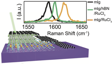
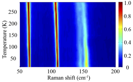
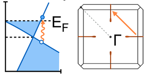
Two-dimensional nanoelectronics, plasmonics, and emergent phases require clean and local charge control, calling for layered, crystalline acceptors or donors. Our Raman, photovoltage, and electrical conductance measurements combined with ab initio calculations establish the large work function and narrow bands of α-RuCl3 enable modulation doping of exfoliated single and bilayer graphene, chemical vapor deposition grown graphene and WSe2, and molecular beam epitaxy grown EuS. We further demonstrate proof of principle photovoltage devices, control via twist angle, and charge transfer through hexagonal boron nitride. Short-ranged lateral doping and high homogeneity are achieved in proximate materials with a single layer of α-RuCl3. This leads to the best-reported monolayer graphene mobilities at these high hole densities and yields larger charge transfer to bilayer graphene.


