
Research
Motivation: The dynamic world is characterized by the flow (reversible) and dissipation (irreversible) of energy, processes that originate from dynamic interactions among electrons, ions, and the environment. Accelerated discovery and design of electronic materials that affords efficient energy utilization therefore requires coherent integration of methods to effectively quantify and engineer the charge and energy transport across different time and length scales. However, there remains critical gaps between fundamental understandings of atomic-level structural details and scalable practical applications, between isolated experimental probes and the complexity of emerging correlated phenomena, and between snapshots of quenched structures and dynamic processes occurring in real time.
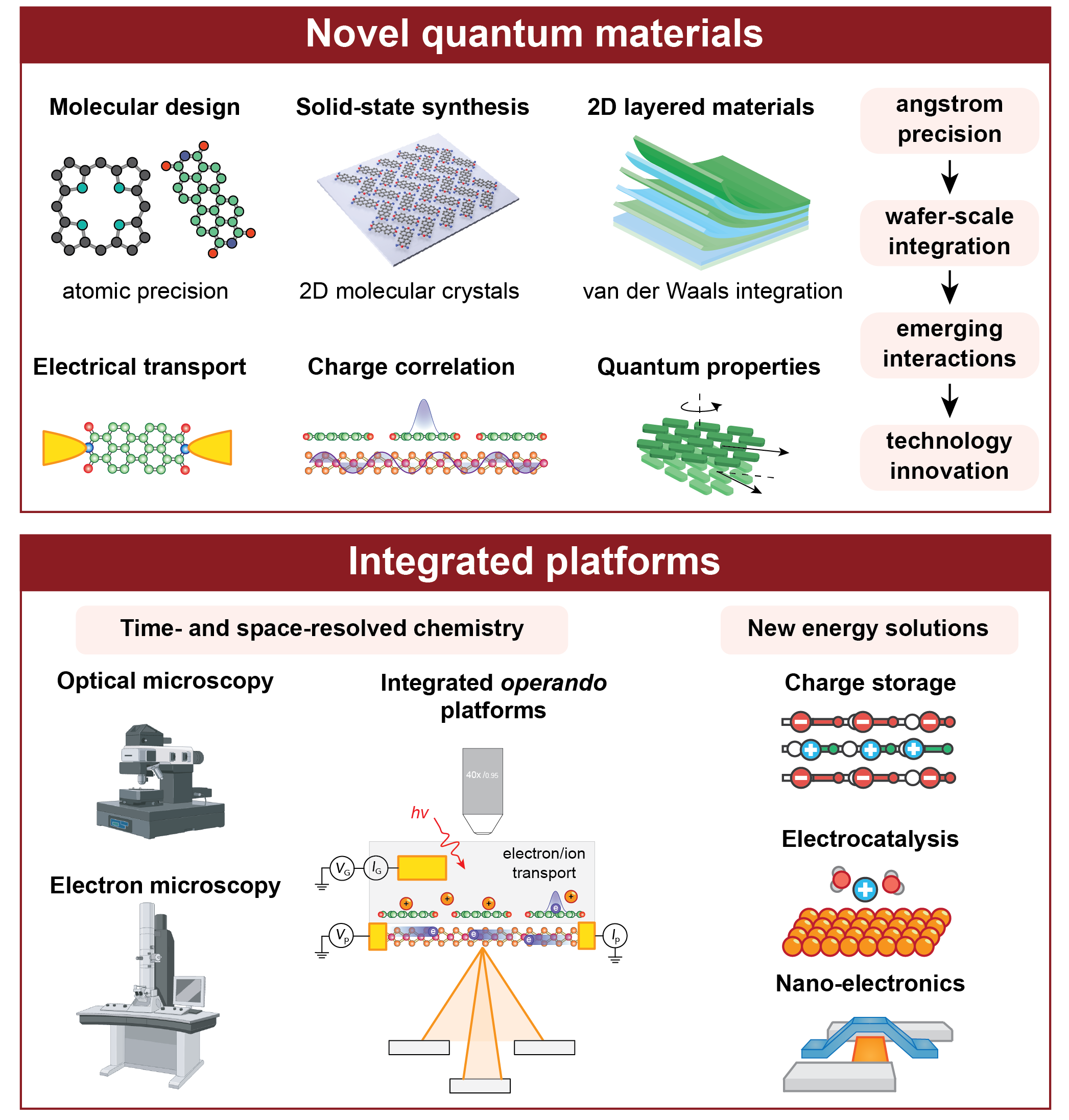
Goal: Our research aims to address this challenge by leveraging advances of nanotechnology, including materials processing, characterization, electron transport, and device integration, to discover electronic materials that host molecular degree of freedom, with their dynamic energy and electron transport behaviors probed in situ. Central to this goal is the investigation of dynamic processes at the electrified interfaces and their correlative connections with application-relevant functions and performance. To accelerate discovery, we integrate higher-level automation and data-driven workflows that enable rapid synthesis, characterization, and analysis across a wide range of electronic and energy systems.
Approaches: We develop new synthetic methods for hybrid molecular solids, where molecular species are coherently incorporated inside extended covalent solids. Our research on hybrid halide perovskites (JACS 2019, 2020, 2022, 2023) and molecule-semiconductor hybrid crystals (Science 2025, ACS Nano 2025) demonstrate the promise of such systems as platforms for discovering unprecedented structural, electrical, optical, and electrochemical properties owing to the intricate interactions between localized molecular orbitals and extended electronic bands. This opens new opportunities for designing energy and semiconductor materials with tailored electronic and ionic properties, enabling energy and integrated electronic applications.
To discover materials with new properties, we develop integrated in situ platforms, enabling multiscale and dynamical structure/property interrogation, that informs better synthetic routes with in-situ feedback and automation. We combine cutting-edge in situ transmission electron microscopy (Nature Nano. 2024, JACS 2023) and electron transport measurement (Science 2025) to design better measurement systems that bridge molecular-level structural insights with mesoscopic device properties. Such platforms will enable the rational design of materials and interfaces for next-generation energy conversion and storage systems, as well as neuromorphic and other unconventional computing architectures that exploit coupled electron-ion dynamics. Ultimately, these integrated approaches will accelerate high-throughput materials discovery and establish feedback-driven principles for chemical innovation and energy applications.